Nanowires are defined as wires with width below 100 nm but they can be several micrometers long. Different techniques are used to fabricate Nanowires: One method is to fabricate the desired material on top of a two-dimensional electron gas to isolate a wire structure. Nanowires can also be chemically produced from a supersaturated solution via the vapor-liquid-solid method. Additionally, particles can be grown from solution and by adhesion of ligands on defined crystal orientations those orientations are prevented from growing further while enabling growth only on orientations without ligands. Another kind of nanowires are carbon nanotubes (CNT) which are simply said rolled up graphene sheets.
In our group we study electrical properties of nanowires and their sensitivity to environmental influences. Our research focuses mainly on CuS-nanorods and CNT-MOF-hybrid structures which were synthesized by our cooperation partner, the Institute of Physical Chemistry and Electrochemistry and the Institute of Inorganic Chemistry.
CuS-Nanorods
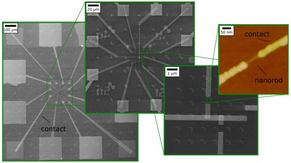
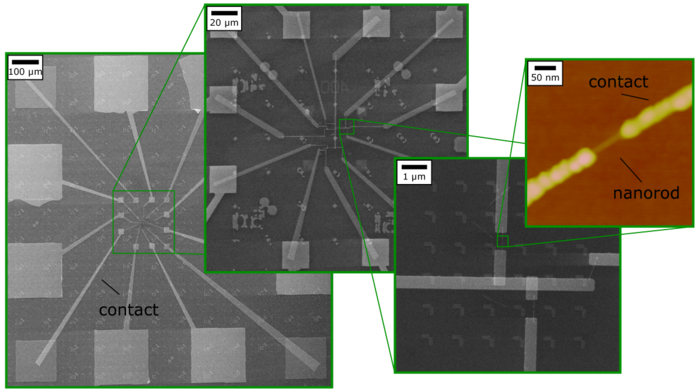
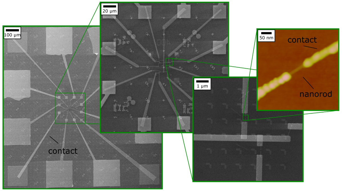
Nanoparticle can consist of many different materials and be chemically synthesised in numerous different geometries. For the integration of nanoparticles in actual application like electronic devices the properties of individual particles are important. In our group the electrical properties of chemically synthesized CuS-nanorods are investigated. Therefor the nanorods are individually contacted with electron beam lithography. In cooperation with the Institute of Physical Chemistry and Electrochemistry the chemical on-chip transformation from contacted CdS- to CuS-nanorods are performed. This allows the transformation from an insulating to a conductive nanoparticle and the direct observation of the changed electrical properties.
 ©
AG Haug
©
AG Haug
CNT-MOF-hybrid structures
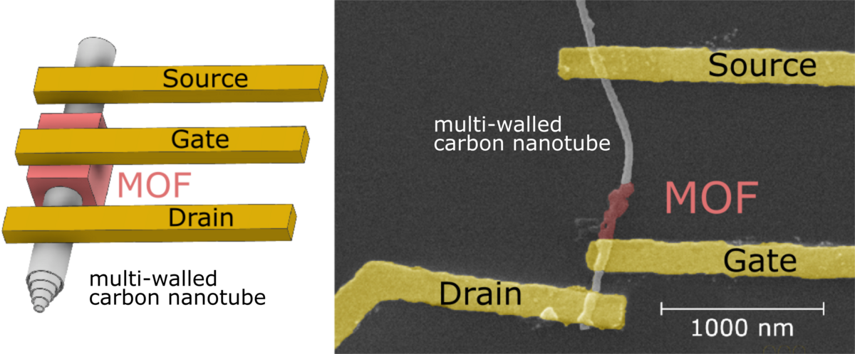
Novel nanometer sized sensing devices can be realized by using metal-organic frameworks (MOFs). MOFs are very porous and highly modular materials for example the pore size can be tuned. Adsorptions in the pores lead to property changes which enable the sensing abilities. An intuitive way of integrating sensors in electrical circuits is to measure resistivity changes. Since most MOFs are nonconducting a state-of-the-art approach is to use networks of carbon nanotubes as conductive carrier medium and measure the influence of the MOF on the nanotubes. To understand the coupling mechanism between carbon nanotubes and MOFs we study in corporation with the Institut für Anorganische Chemie the properties of individual multi-walled carbon nanotubes with UiO-66 MOF on them.


 ©
AG Haug
©
AG Haug