Insulating thin films and their applications
Wide band gap insulators are ubiquitous in nature, mostly as crystalline minerals. Although in general chemically apparently inert, at least as perfect stoichiometric substances, their use as template materical in catalysis and their interplay with the catalytically active material is a matter of active research at present.
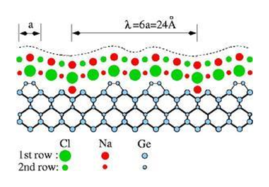
Our attempts to grow selected substances as epitaxial crystalline thin films focusses on mainly two other aspects. Insulators serve of course as embedding material for all kinds of electric conductors or as spacers between conducting plates forming a capacitor. In both cases the electronic states at the interface play a crucial role. These can best studied and manipulated in a crystalline insulating layer. Band gaps can be tailored and defect densities be adjusted by use of mixed oxides that allow adjustment of the lattice constants between substrate and insulating crystalline film. Defects, on the other hand, act as electronic traps, but also determine the band alignment between insulator and a semiconductor, e.g. Their density can be also manipulated by structural modifications (by steps, e.g.) and by controlled insertion of impurities and vacancies.
Structural modifications can be obtained by varying growth parameters in epitaxy, but, for crystalline growth, also by use of vicinal substrates. In some cases perfect replicas of the step morphology in the insulator are obtained. Due to their higher coordination, the steps in the insulator can serve as nucleation centers for further (metallic) structures on top.
On the other hand, anion vacancies at the surface of an insulating film provide electronic surface states, which are positioned in the band gap of the insulator. Due to their excitation in the optical frequency range, they are known as color centers. Their much lower energy compared to the excitation of excitons or free carriers, they act as chemically active sites. The generation of such active sites, the study of their excitation mechanisms, and their function as nucleation sites for ultra-small dots and wires is included in our research.
As part of Molecular Electronics, adsorption of organic molecules on insulators, both on perfect and defect-rich surfaces, offers a possibility to tailor band gaps at the surface (see schematic). This has important implications not only in nanoelectronics with ultra-small structures in the range of a few nanometers, but also in such basic processes like contact charging.
Selected publications:
S. Islam, D. Müller-Sajak, K. R. Hofmann, H. Pfnür (2013): Epitaxial thin films of BaSrO as gate dielectric, Microelectronic Engineering 109, 152 (2013)
DOI: 10.1016/j.mee.2013.03.105
D. Müller-Sajak, S. Islam, H. Pfnür, K.R. Hofmann (2012): Temperature stability of ultra-thin mixed BaSr-oxide layers and their transformation, Nanotechnology 23, 305202 (2012)
DOI: 10.1088/0957-4484/23/30/305202