The courses are conducted following our set of laboratory rules(english version in preparation). Further questions can be addressed to Dr. Tammo Block (Room: 257, block@maphy.uni-hannover.de).
We hope you will have an interesting and successful time!
The Academic Staff of the Institute for Solid State Physics
Dates for winter term
The assignment of different experiments for students is carried out via StudIP.
The assignment and notification of master students ensues via email after the assignment of bachelor students.
Please see the german page for the dates.
Dates for summer term
The assignment of different experiments for students in their bachelor and master program is carried out after the enrollment via StudIp in summer term.
You will receive a notification email after the beginning of the lecture period.
Please see the german pages for the dates.
Experiment descriptions and instruction manuals
-
Resonate Tunnel Diodes
Focus of this experiment is the examination of resonant tunneling diodes. In contrast to the classical understanding resonant tunneling diodes given by a double barrier structure allow tunneling of charge carriers through thin barriers.
During this training resonant tunneling diodes manufactured of semiconductor materials (GaAs/AlAs) should be examined for several temperatures between room temperatures and 4.2 K. Different properties of resonant tunneling diodes will be determined with the help of current-voltage characteristic.
Person of contact: Maximilian Mischke
![]()
![]()
![]()
-
X-Ray photoemission spectroscopy
The morphology and electronic properties of interfaces and surfaces are analyzed using various methods (e.g. XPS, UPS, LEED, STM, AFM). Photoelectron spectroscopy (XPS, UPS) is one of the most important methods for examining the chemical composition, the bonding relationship and the electronic properties of interfaces and surfaces. Depending on the excitation energy of the light source, a distinction is made between UPS ("Ultraviolet Photoelectron Spectroscopy") hv = 5eV to 41eV and XPS ("X-Ray Photoelectron Spectroscopy") hv = 100eV to 1500eV. The information depth of this method is only between 5Å and 30Å , which corresponds to about 2 to 15 atomic layers. On the other hand, this dependency can be used specifically to study the layer thickness of adsorbates, for example. In addition to determining the binding energy of primary structures, secondary effects such as e.g. ghost peaks, shake-up, shake-off, will be studied in more detail.Anleitung
Kontaktperson: Frederik Bettels
![]()
![]()
![]()
-
Analysis of the current-voltage characteristics of solar cells
In this experiment, you analyze industrially manufactured silicon solar cells using measured current-voltage characteristics (I-V curves). You will learn about the functionality of silicon solar cells and gain experience in the field of semiconductor physics. Furthermore, you will get to know the LabView programming environment, which is used in many scientific and industrial applications. In the first part of the experiment, you will measure the I-V characteristic of the solar cell in the dark to investigate its recombination properties. Then you measure the I-V curve under illumination to determine and interpret the efficiency and some other parameters. In order to be able to record the characteristic curves computer-controlled, you program the control of the measurement setup yourself in LabView. For the execution of the experiment you have measuring equipment at your disposal, as it is used in research laboratories and industry.
Person of contact: Tobias Wietler
![]()
![]()
![]()
-
Analysis of the angle-dependent spectral luminescence emission of silicon wafers
Luminescence emission in solar cells is the reverse process of absorption of light under generation of electrical charge carriers. The analysis of the luminescence emission provides information about various properties of the investigated sample, such as the temperature of the sample, recombination of charge carriers, local voltage or surface roughness.
In this experiment you will analyze the electro- and photoluminescence emission of silicon solar cells and silicon wafers both spectrally resolved using a spectrometer and spatially resolved using a camera. You will get to know the functionality of silicon solar cells and gain experience in the field of semiconductor physics. You will also learn how to work with diode array spectrometers and scientific silicon CCD cameras. For the execution of the experiment you will be provided with measuring equipment as used in research laboratories and industry.
Person of contact: Tobias Wietler
![]()
![]()
![]()
-
Analysis of the quantum efficiency of solar cells
The quantum efficiency of solar cells describes what proportion of the photons hitting the solar cell produce electron-hole pairs, which contribute to the generated electric current. It is thus a measure of both optical and electrical losses that occur in the solar cell. The determination of the quantum efficiency for different wavelengths also provides information about the electrical and optical properties of different areas of the solar cell. For this reason, the measurement of the quantum efficiency is an important characterization method that is widely used in photovoltaic research and industry. In this experiment you determine the quantum efficiency of different solar cell types and interpret the measurement curves. In doing so, you will get to know how silicon solar cells work and gain experience in the field of semiconductor physics. To carry out the experiment, you will be provided with measuring equipment as used in research laboratories and industry.
Person of contact: Tobias Wietler
![]()
![]()
![]()
-
Spin dynamic of semiconductors
This experiment provides general knowledge in the fields of semiconductor physics, optics and spin dynamics at low temperatures. The general objective is to optically measure the lifetime of an optical spin excitation in a lightly doped semiconductor under the influence of a magnetic field. In the first part of the experiment the optical and polarization resolving components are aligned. Subsequently you cool down the semiconductor sample to the temperature of helium and perform the measurements at low temperatures. The intensity and polarization of the excited photoluminescence is anlyzed in dependence of an externally applied magnetic field. This method is known as Hanle depolarization measurement.
Person of contact: Nico Eggeling
![]()
![]()
![]()
-
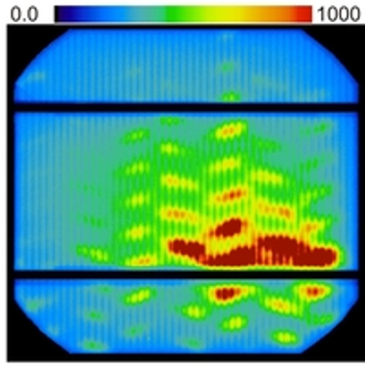
Quantum Hall Effect
The quantum Hall effect is one of the fundamental phenomena occurring in two-dimensional electron systems. Although it has been investigated for more than three decades we are still far away from complete understanding of this effect. Especially, the theory of the fractional quantum Hall effect is challenging so that not every experiment is understood until now.
During this training you get an idea of the physics behind the quantum Hall effect, including an overview of the theory and a short introduction of the sample preparation. The properties of the considered heterostructures should be analyzed with the help of magnetotransport measurements at low temperatures.
Person of contact: Bei Zheng
![]()
![]()
![]()
-
Determination and modification of the surface morphology with an atomic force microscope
An atomic force microscope (AFM) is used to examine the morphology of various surfaces in air. The AFM doesn't offer the high resolution of a scanning tunneling microscope, but it also enables the examination of non-conductive materials on an atomoic scale.
The first part of the experiment is used to familiarize yourself with this highly sensitive measuring method. In the second part, the step structure of non-conductive ion crystals and the change in the surface due to the surrounding atmosphere ca be determined, and the defects can be introduced and measured in a targeted manner.
Contact: Ilija Funk
![]()
![]()
![]()
-
Solid-state nuclear magnetic resonance
The solid-state nuclear magnetic resonance (NMR) was discovered nearly simultaneously by E. Purcell and F. Bloch with different apparatuses. The discovery led to spectroscopic methods which are still used by physicists, chemists, geologists and biologists to gain detailed knowledge of the microscopic structure of matter. For this a sample is placed in a magnetic field and irradiated by electromagnetic waves with determined energy and intensity. The radiation induces transitions between nuclear states of the material which are subsequently detected electrically. Only physical requirement for this method is a nuclear spin unequal zero.
In this experiment you will independently work out the fundamental principles of nuclear magnetic resonance and will collect practical laboratory experience with a pulsed NMR spectrometer. Furthermore the investigation of the spatial structure of individual samples is possible.Person of contact: Kai Hühn
![]()
![]()
![]()
-
Determination of the surface morphology with a scanning tunneling microscope
A scanning tunneling microscope (STM) is used to examine various surfaces in air for their morphology. A gold layer and a graphite crystal with a freshly prepared surface are evailable for testing. On the graphite surface an atomic resolution can even be achieved in air. In the further course of the experiment, other surfaces (partly in ultra-high vacuum) should be prepared in a targeted manner and then characterized with the STM.
Contact person: Denis Uhland
![]()
![]()
![]()